Fermi Level In Semiconductor / Types of Semiconductors
Fermi Level In Semiconductor / Types of Semiconductors. A semiconductor is a solid that is defined as having its fermi level (chemical potential) in a band gap of the electronic structure of the solid, which is not too large compared to the thermal energy, so that, according to the fermi distribution, at room temperature you have a significant number of electrons and/or holes in the conduction and. The added impurity is very small, of the order of one atom. • at o k no conduction because at o k valence band is completely filled while conduction band empty and semiconductor behave as insulator. Above is a diagram (ref. Kb is the boltzmann constant.
ads/bitcoin1.txt
Semiconductor doping and higher temperatures can greatly improve the conductivity of the pure semiconductor material. The fermi level is the energy separating occupied states of the valence band from empty states of the conduction band at the absolute temperature t=0 kelvin. There are many (or too many) references on the subject because of its importance. Kb is the boltzmann constant. Fermi level of intrinsic semiconductor those semi conductors in which impurities are not present are known as intrinsic semiconductors.
nanoHUB.org - Courses: ECE 606: Solid State Devices ... from nanohub.org 1.1 0, indicating equal concentrations of electrons and holes. Fermi level is a kind of measure of equilibrium electronic energy of a solid material. Kb is the boltzmann constant. Whenever the system is at the fermi level, the population n is equal to 1/2. The fermi level is the energy separating occupied states of the valence band from empty states of the conduction band at the absolute temperature t=0 kelvin. Semiconductor doping and higher temperatures can greatly improve the conductivity of the pure semiconductor material. The correction term is small at room temperature since eg ~ 1 ev while kbt ~ 0.025 ev. There are many (or too many) references on the subject because of its importance.
For si and ge, nc > nv and the correction term is negative while for gaas nc < nv and the correction term is positive.
ads/bitcoin2.txt
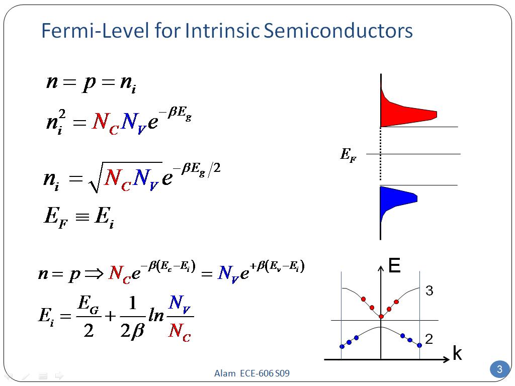
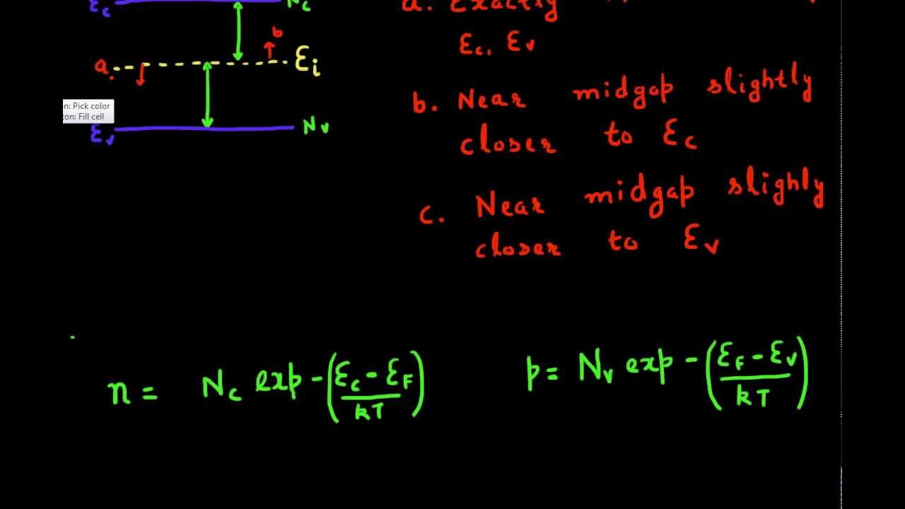
Fermi level is a kind of measure of equilibrium electronic energy of a solid material. If you can bring the fermi level high enough, then part of the tail will go over to the conduction band. The correction term is small at room temperature since eg ~ 1 ev while kbt ~ 0.025 ev. The fermi level pinning effect is strong in many commercially important semiconductors (si, ge, gaas), and thus can be problematic for the design of semiconductor devices. Kb is the boltzmann constant. This probability of occupation of energy levels is represented in terms of fermi level. For si and ge, nc > nv and the correction term is negative while for gaas nc < nv and the correction term is positive. The fermi level plays an important role in the band theory of solids. Ec is the conduction band. Position of fermi level in intrinsic semiconductors • width of conduction band and valence band is small as compared to forbidden energy gap. The fermi level in a semiconductor is one of the most parameters in understanding and modeling (now using computers) the electrical behaviors of all the semiconductors we are currently interested in. The fermi level is referred to as the electron chemical potential in other contexts. K.consequently, we see from this equation that the fermi level should typically lie very close to the middle of the energy gap in intrinsic semiconductors.
The fermi level is the surface of fermi sea at absolute zero where no electrons will have enough energy to rise above the surface. For si and ge, nc > nv and the correction term is negative while for gaas nc < nv and the correction term is positive. At absolute zero temperature intrinsic semiconductor acts as perfect insulator. I can understand that the distribution changes with the temperatures (it gets broader) but i don't understand why/how the fermi level changes. T is the absolute temperature.
Fermi Level in Extrinsic Semiconductor - Theory & effect ... from i.ytimg.com Ev, while the second is of the order of a few tens of millielectron volts at 300. Where the fermi energy is located (correct?). T is the absolute temperature. I can understand that the distribution changes with the temperatures (it gets broader) but i don't understand why/how the fermi level changes. The correction term is small at room temperature since eg ~ 1 ev while kbt ~ 0.025 ev. Due to lack of sufficient energy at 0 kelvin, the fermi level can be considered as the sea of fermions (or electrons) above which no electrons exist. • all energy level in one band is same energy. In a perfect semiconductor (in the absence of impurities/dopants), the fermi level lies close to the middle of the band gap 1.
Kb is the boltzmann constant.
ads/bitcoin2.txt
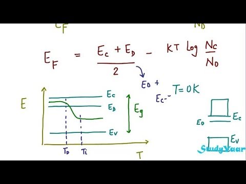
This probability of occupation of energy levels is represented in terms of fermi level. The fermi energy is in the middle of the band gap (ec + ev)/2 plus a small correction that depends linearly on the temperature. However as the temperature increases free electrons and holes gets generated. Fermi level is a kind of measure of equilibrium electronic energy of a solid material. Fermi level of extrinsic semiconductor extrinsic semiconductors are formed by adding suitable impurities to the intrinsic semiconductor. Fermi level of intrinsic semiconductor those semi conductors in which impurities are not present are known as intrinsic semiconductors. Semiconductor doping and higher temperatures can greatly improve the conductivity of the pure semiconductor material. If you can bring the fermi level high enough, then part of the tail will go over to the conduction band. Due to lack of sufficient energy at 0 kelvin, the fermi level can be considered as the sea of fermions (or electrons) above which no electrons exist. At absolute zero temperature intrinsic semiconductor acts as perfect insulator. Where the fermi energy is located (correct?). 1.1 0, indicating equal concentrations of electrons and holes. The fermi level represents the electron population at energy levels and consequently the conductivity of materials.
Kb is the boltzmann constant. The fermi level pinning effect is strong in many commercially important semiconductors (si, ge, gaas), and thus can be problematic for the design of semiconductor devices. Fermi level ef to me is the reference level to measure the concentration of electrons or holes in a semiconductor. I can understand that the distribution changes with the temperatures (it gets broader) but i don't understand why/how the fermi level changes. If you can bring the fermi level high enough, then part of the tail will go over to the conduction band.
Position of Fermi level in instrinsic semiconductor - YouTube from i.ytimg.com Kb is the boltzmann constant. The fermi level lies between the valence band and conduction band because at absolute zero temperature the electrons are all in the lowest energy state. We show that this problem can be overcome by using 2d. If you can bring the fermi level high enough, then part of the tail will go over to the conduction band. Fermi level lies in the midway between the valence band top and conduction band bottom of an intrinsic semiconductor, as shown in fig. Fermi level is a kind of measure of equilibrium electronic energy of a solid material. Semiconductor doping and higher temperatures can greatly improve the conductivity of the pure semiconductor material. Due to lack of sufficient energy at 0 kelvin, the fermi level can be considered as the sea of fermions (or electrons) above which no electrons exist.
The electrical conductivity of the semiconductor depends upon the total no of electrons moved to the conduction band from the valence band.
ads/bitcoin2.txt
Ev, while the second is of the order of a few tens of millielectron volts at 300. Kb is the boltzmann constant. A semiconductor is a solid that is defined as having its fermi level (chemical potential) in a band gap of the electronic structure of the solid, which is not too large compared to the thermal energy, so that, according to the fermi distribution, at room temperature you have a significant number of electrons and/or holes in the conduction and. For si and ge, nc > nv and the correction term is negative while for gaas nc < nv and the correction term is positive. Fermi level is a kind of measure of equilibrium electronic energy of a solid material. There are many (or too many) references on the subject because of its importance. The electrical conductivity of the semiconductor depends upon the total no of electrons moved to the conduction band from the valence band. (18) is of the order of 1. Fermi level of intrinsic semiconductor those semi conductors in which impurities are not present are known as intrinsic semiconductors. Green, unsw) illustrating the location of the fermi level e f relative to the valence and conduction bands for various materials. The added impurity is very small, of the order of one atom. The fermi level is the level where the probability that an electron occupies the state is 0.5, e.g. T is the absolute temperature.
ads/bitcoin3.txt
ads/bitcoin4.txt
ads/bitcoin5.txt
0 Response to "Fermi Level In Semiconductor / Types of Semiconductors"

0 Response to "Fermi Level In Semiconductor / Types of Semiconductors"
Post a Comment